Wafers Unlimited
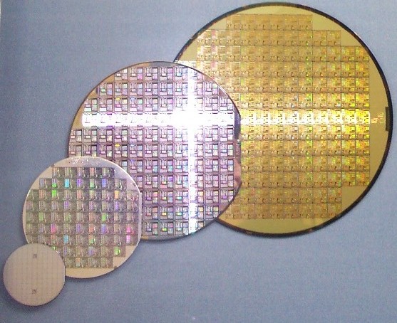
DESO Technology Limited (Hong Kong), a trading company, offers a wide spectrum of semiconductor wafers. We offer Silicon wafers, Germanium wafers, Gallium Nitrate (GaN) wafers, Silicon Carbide (SiC) wafers, Gallium Arsenide (GaAs) wafers, Cadmium Zinc Telluride (CdZnTe or CZT) wafers, Sapphire (Aluminium Oxide Al2O3) wafers, and compound wafers (Indium Phosphate InP, Indium Arsenide InAs, Indium Antimonide InSb, Gallium Antimonide GaSb).
Waffer Process:
Wafer Crystal Growth: Single crystal growth is an essential first stage in the production of crystal wafers. creating ingots in a sealed furnace using polycrystals as the raw material and a small amount of dopant, such as nitrogen, vanadium, boron, or phosphorus. The resistivity, or electrical characteristics, of the wafers that are cut from the crystal are determined by the dopant.
Wafer Cutting: To best prepare the ingot for the slicing process, the seed-end (the top) and the tappered-end (the bottom) of the ingots are removed. Then the ingot is cut into shorter sections. Subsequently, each section is ground to the specified diameter in a mechanical lathe, and the crystals are cut into wafer slices.
Wafer Polishing: First step consists of rough smoothing by Mechanical polishing. Second step consists of fine smoothing by CMP (Chemical Mechanical Polishing) to improve the wafer flatness and surface roughness, so that it emerges epi-ready.
Wafer Cleaning: Wafers are then inspected for scratches, spots and inclusions. The conforming wafers undergo cleaning by going through several specialized wafer cleaning machines.
Wafer Epitaxy: Epitaxy is the process of crystal growth in which new crystalline layers are formed, by reactor, with one or more well-defined orientations with respect to the crystalline seed layer. The end-product is an epiwafer, that may serve as a substrate (wafer) for compound semiconductor devices.
Epitaxy technological capabilities:
- Hydride Vapour Phase Epitaxy (HVPE): Applicable to GaN, AIN, AlGaN, and other compound semiconductors. Have wide area of applications, including solid state lighting, short wavelength optoelectronics, and RF power devices.
- Molecular Beam Epitaxy (MBE): A method of depositing layers of material with atomic thicknesses onto the substrate. A ‘molecular beam’ of material is created and is etched onto the substrate. Resulting ‘superlaticces’ have a number of critical applications including Quantum Well lasers, Giant Magneto-Resistance for metallic systems, and optimal for microwaves and RF applications. Typically the epitaxial layers are grown on GaAs or other compound semicondutor substates.
- Metal Organic Chemical Vapor Deposition (MOCVD) or Metal-Organic Vapor Phase (MOVPE): A chemical vapour deposition technique for epitaxy by depositing atoms on a wafer substrate. Atoms that the user wants to be included in the crystal are joined with complex organic gas molecules and passed over a hot wafer surface. The heat breaks the large molecules and deposits the desired atoms onto the surface, layer by layer. By altering the composition of the gas, we can modify the properties of the crystal at almost the atomic scale. This technique is capable of growing ultra high quality semiconductor layers where the crystal structure of each layer is perfectly aligned with that of the substrate.
For quotations and questions please contact: Admin@WafersUnlimited.com
