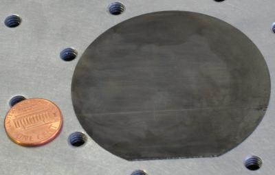
DESO Technology Limited (Hong Kong) Germanium Wafers
DESO Germanium (Ge) offers 2 inches diameter wafers.
Ge wafers are grown using VGF/LEC method. Lightly doped P and N type Ge wafers may be used for Hall effect experiments. Ge serves as a semicondutor. High-purity Germanium is doped with trivalent elements (e.g. indium, gallium, boron) to construct P-type Ge semicondutors; and doped with pentavalent elements (e.g. antimony, arsenic, phosphorus) to construct N-type Ge semiconductors. Germanium has excellent semincondutor properties including high electron mobility and mole mobility.
Product Specifications
General Properties Structure |
Cubic, a=5.6754 Angstrom |
Crystal Growth Technology: Czechrolaski
Doping Available |
None |
Sb Doping |
Doping In / Ga |
Conductive Type |
N |
N |
P |
Resistivity, Ohm*cm |
>35 |
<0.05 |
0.05 – 0.1 |
EPD, max. |
<5 x 10^3 /cm^2 |
<5 x 10^3 /cm^2 |
<5 x 10^3 /cm^2 |
EPD, min. |
<5 x 10^2 /cm^2 |
<5 x 10^2 /cm^2 |
<5 x 10^2 /cm^2 |
Grade |
Application |
Electronic |
Diodes and Transistors |
Infrared or Optical |
IR optical window, disks, or components |
Cell |
Solar cell |
Parameter |
Specification |
Comment |
Growth Method |
VGF |
|
Conduction Type |
n-type, |
|
Dopant |
Gallium or Antimony |
|
Wafer Diameter |
2 |
inches |
Crystal Orientation |
(100),(111),(110) |
|
Thickness |
200 – 550 |
um |
OF |
EJ or US |
|
Carrier Concentration |
upon customer request |
|
Resistivity at RT |
0.001 – 80 |
Ohm*cm |
Pit Density |
<5000 |
/cm^2 |
Laser marking |
upon request |
|
Surface finish |
P/E or P/P |
|
Epi ready |
Yes |
|
Package |
Single wafer container or cassette |
For quotations and questions please contact: Admin@WafersUnlimited.com
