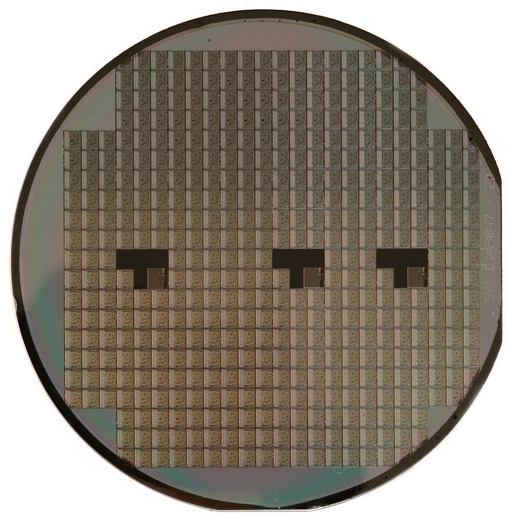
DESO Technology Limited (Hong Kong) Silicon Wafers
DESO offers 12 inches diameter Thermal Oxidation (Si) wafers.
Thermal oxide/dioxide silicon wafer is a bare silicon wafer with oxide layer grown via dry/wet oxidation process. Thermal oxide layer is typically gorwn in a horizental tube furnace, at temperature ranging from 900 to 1200 C. In comparison to CVD grown oxide layer, Silicon oxide layer grown by thermal oxidation has higher uniformity, compactness, dielectric strength and quality overall.
Product Specifications
Parameter |
Value |
Type of ingot |
Grown according to Czochralski method |
Diameter, mm |
300 +/- 0.2 |
Wafer Lifetime, months |
12 |
Dopant |
B (boron) |
Conductivity type |
P |
Oxigen max, OLD – PPMA |
40 |
Carbon, PPMA |
1 |
Exclusion of the edge zone, mm |
3 |
Crystallographic orientation |
<100> |
Deviation from the predetermined surface orientation of crystal plane, degrees |
0.5 |
Volume resistivity, Ohm * cm |
10-40 |
Number of dislocations, cm^-2 |
0 |
Number of point etching defects, cm^-2 |
0 |
Number of point oxidation defects, cm^-2 |
500 |
Maximum iron content in the volume, E10AT/CC |
10 |
Primary Notch |
Yes |
Notch location |
110 |
Notch size, mm |
2.3 |
Notch Form |
V |
Wafer thickness, microns |
775 +/- 25 |
Type of marking |
Laser |
Marking Location |
back side |
Edge profile |
by SEMI T/4 |
Scratches on the front side |
absent |
Total change in wafer thickness (TTV), microns |
5 |
Deflection (WARP), microns |
60 |
The number of particles on a surface larger than 0.09 microns |
50 |
Contamination of the back side |
absent |
Surface content of aluminum, E10AT/CM2 |
1 |
Surface content of calcium, E10AT/CM2 |
1 |
Surface content of chromium, E10AT/CM2 |
1 |
Surface content of copper, E10AT/CM2 |
1 |
Surface content of iron, E10AT/CM2 |
1 |
Surface content of potassium, E10AT/CM2 |
1 |
Surface content of natrium, E10AT/CM2 |
1 |
Surface content of nickel, E10AT/CM2 |
1 |
Surface content of zinc, E10AT/CM2 |
1 |
Requirements to accuracy of flatness, microns |
0.3 |
Exclusion of the edge zone when measuring flatness, mm |
3 |
Packing Requirements:
| Parameter | Value |
| Type of Packaging | MW300GT-A |
| Inner Container Material | Polyethylene |
| Outer Packing Material | Aluminum |
| Number of units per packages | 25 |
| Reusability | Yes |
Oxidation Methods
Dry oxidation: Dry oxygen oxidation Silicon reacts with Oxygen at a temperature of 850 to 1200 degrees Celsius. Although the rate of thermal oxide growth is low, very high quality is maintained. This approach can be applied for MOS insulate gate growth. Silicon wafer oxide thickness manufactured by this process ranges from 10 nm to 300 nm.
Wet oxidation: At high temperature, water vapor enters the furnace tube and forms an oxide layer on the surface of the silicon wafer. The density of wet oxygen oxidation is marginally worse than that of dry oxygen oxidation, however it has a higher growth rate. This approach is ideal for growing films with thickness above 500 nm. Wet oxidation capacity: 100 nm – 6 um.
The result of wet/dry oxidation process, a Silicon oxide wafer layer has high electrical resistivity and would easily store electrical energy, functioning as an optimal insulator. In a number of silcon-based devices, thermal oxide layers have a critical role in doping prevention and surface dielectric.
For quotations and questions please contact: Admin@WafersUnlimited.com
